 |
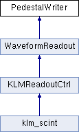
Belle II KLM Scint Firmware
1
|
 |
Belle II KLM Scint Firmware
1
|

Entities | |
| Behavioral | architecture |
Libraries | |
| IEEE | |
| work | |
Use Clauses | |
| STD_LOGIC_1164 | |
| NUMERIC_STD | |
| STD_LOGIC_MISC | |
| STD_LOGIC_UNSIGNED | |
| klm_scint_pkg | Package <klm_scint_pkg> |
Generics | |
| PED_RAM_tSCE_g | integer := 6 |
| PED_RAM_tLZWE_g | integer := 20 |
| PED_RAM_tSA_g | integer := 1 |
| PED_RAM_tHA_g | integer := 1 |
Ports | |
| clk | in STD_logic |
| ena | in std_logic_vector ( 1 downto 0 ) := ( others = > ' 0 ' ) |
| ack | out std_logic_vector ( 1 downto 0 ) := ( others = > ' 0 ' ) |
| asic_addr | in slv3 ( 1 downto 0 ) |
| chan_addr | in slv4 ( 1 downto 0 ) := ( others = > " 0000 " ) |
| win_addr | in std_logic_vector ( 8 downto 0 ) := ( others = > ' 0 ' ) |
| samp_addr | in slv4 ( 1 downto 0 ) := ( others = > ( others = > ' 0 ' ) ) |
| even_sample | in slv12 ( 1 downto 0 ) := ( others = > ( others = > ' 0 ' ) ) |
| odd_sample | in slv12 ( 1 downto 0 ) := ( others = > ( others = > ' 0 ' ) ) |
| RAM_din | out std_logic_vector ( 7 downto 0 ) := ( others = > ' 0 ' ) |
| RAM_WEb | out std_logic := ' 1 ' |
| RAM_ADDR | out std_logic_vector ( 21 downto 0 ) := ( others = > ' 1 ' ) |
Part: CY62177EV30
Write to the pedestal ram. Input is even hardware address (note that LSB of samp_addr is intentionally omitted), plus two consecutive sample values (starting with the even-addressed sample). This module is initiated with an enable signal, and sends an acknowledge signal when it's finished. The scope is for servicing two busses, so all inputs (plus ack output) are bussed in parallel, and a trivial arbiter decides which bus to service (always give priority to first bus in order to keep logic minimal)
| BUS | ASIC | CH | WIN | SAMP |
|---|---|---|---|---|
| 1 | 3 | 4 | 9 | 5 |
4M addresses available, 8 bits values. 10 ASIC * 16 CH * 512 WIN * 32 SA * 1.5 bytes/SA = 3,932,160 bytes This requires storing 2 peds across 3 addresses, and requires using TXDC.
/|  TXDC   |   CH    |          WIN          |    SAMP   |\
||----4----|----4----|-----------9-----------|-----5-----|| * 1.5 + (0|1|2)
\|---------|---------|-----------------------|-----------|/
### RAM Write-Cycle clock diagram*
clk      /‾‾\__/‾‾\__/‾‾\__/‾‾\__/‾‾\__/‾‾\__/‾‾\__/‾‾\__/‾‾\__/‾‾\__/‾‾\__/
RAM_addr ‾_‾_‾_╳_‾_‾_‾_‾_‾_‾_‾_‾_‾_‾_‾_‾_‾_‾_‾_‾_‾_‾_‾_‾_‾_‾_‾_‾_‾_‾_╳_‾_‾_‾
RAM_din  ‾_‾_‾_╳_‾_‾_‾_‾_‾_‾_‾_‾_‾_‾_‾_‾_‾_‾_‾_‾_‾_‾_‾_‾_‾_‾_‾_‾_‾_‾_╳‾_‾_‾_
RAM_WEb  ‾‾‾‾‾‾\_______________________/‾‾‾‾‾‾‾‾‾‾‾‾‾‾‾‾‾‾‾‾‾‾‾‾‾‾‾‾‾\______
             |<----    T_sce   ----->|
*In writing-mode, should have RAM_rw=0
Definition at line 45 of file PedestalWriter.vhd.